| |
 |
| |
LRW1/LRW2/LRW3
LRW-AES Cores
|
| |
General Description
|
Key Features
|
| |
|
Implementation
of the older drafts standard
IEEE P1619 required the NIST standard AES cipher in the LRW
mode for encryption (AES-LRW). Note that the
new drafts of the P1619 call for a different mode,
XTS-AES (see our XTS cores).
The LRW1 AES core is tuned for storage applications at the data rates of 3 Gbps and higher.
The LRW2 family of cores covers a wide range of area /
throughput combinations, allowing the designer to choose
the smallest core that satisfies the desired
clock/throughput requirements. All LRW cores contain the base AES core AES1 and
are available
for immediate licensing. LRW3 family is similar to
LRW2, but supports 256-bit AES keys and no-penalty key
and IV changes.
The design is fully synchronous and available in both
source and netlist form. |
Small size: LRW1 starts at 30,000 ASIC gates at throughput of
12.8 bits per clock
Synthesized for 600+ MHz clock speeds (70+ Gbps
throughput for LRW2-128)
Completely self-contained: does not require external
memory
Supports Liskov-Rivest-Wagner encryption and decryption
(LRW-AES a.k.a. AES-LRW)
Includes LRW-AES encryption, LRW-AES decryption, key expansion and
data interface
Flow-through design
No penalty for key and IV changes (back-to-back
operation)
128+128 bit LRW keys supported. 256+128 bit key
supported by LRW3.
Easily parallelizable for higher data rates
Test bench provided
|
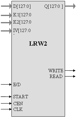
Symbol
|
LRW-AES Applications
|
| |
|
|
|
Storage encryption
|
|
| |
Pin Description
|
| |
|
Name
|
Type
|
Description
|
|
CLK
|
Input
|
Core
clock signal |
|
CEN
|
Input
|
Synchronous
enable signal. When LOW the core ignores all its inputs
and all its outputs must be ignored. |
|
MODE
|
Input
|
Mode.
When HIGH, write (LRW-AES encryption), when LOW, read
(LRW-AES decryption) |
|
START
|
Input
|
HIGH
starting input data processing |
|
READ
|
Output
|
Read
request for the input data byte |
|
DATA_VALID
|
Input
|
HIGH
when valid data byte present on the input |
|
WRITE
|
Output
|
Write
to the output interface |
|
OUT_READY
|
Input
|
HIGH
when output interface is ready to accept data byte |
| D[127:0] |
Input |
Input
Data (plain or cipher text, other data bus widths are also available)
|
|
K1[255:0] |
Input |
AES
key (128-bit key option is also available) |
|
K2[127:0] |
Input |
Tweak
key (K2) |
|
IV[127:0] |
Input |
Logical position (I) |
| Q[127:0] |
Output |
Output
plain or cipher text |
|
| |
Function Description
|
| |
|
The Advanced Encryption Standard (AES) algorithm is a new
NIST data encryption standard as defined in the
http://csrc.nist.gov/publications/fips/fips197/fips-197.pdf
LRW implementation fully supports the AES algorithm
for 128+128 and 256+128 bit keys LRW-AES mode as required by
the P1619 IEEE draft standard.
The cores are designed for flow-through operation, with selectable
width of input and output interfaces. LRW cores
support both encryption and decryption modes.
|
| |
Implementation Results
|
| |
Area Utilization and Performance
|
| |
| Representative area/resources figures are shown
below. |
| |
|
Core |
Technology
|
Area / Resources
|
Max Frequency
|
Throughput
|
|
LRW1 |
TSMC 0.13 µ LV
|
29,959 gates
|
100 MHz
|
1.28 Gbps
|
|
LRW1 |
TSMC 0.09 µ LV
|
60,165 gates
|
600 MHz
|
7.68 Gbps
|
|
LRW2-25.6 |
TSMC 0.09 µ LV |
44,405 gates |
100 MHz |
2.56 Gbps |
|
LRW2-64 |
TSMC 0.09 µ LV |
84,269 gates |
100 MHz |
6.4 Gbps |
|
LRW2-64 |
TSMC 0.09 µ LV |
196,914 gates |
515 MHz |
33 Gbps |
|
LRW2-128 |
TSMC 0.09 µ LV |
150,817 gates |
100 MHz |
12.8 Gbps |
|
LRW2-128 |
TSMC 0.09 µ LV |
311,252 gates |
305 MHz |
39 Gbps |
|
LRW2-128 |
TSMC 0.09 µ LV |
399,208 gates |
550 MHz |
70.4 Gbps |
|
| |
|
Multiple LRW cores can be easily paralleled
for throughputs of 100 Gbps and higher.
|
| |
Export Permits
|
| |
US Bureau of Industry and Security has assigned
the export control classification number 5E002 to our AES
core. The core is eligible for the license exception ENC
under section 740.17(A) and (B)(1) of the export
administration regulations. See the
licensing basics page,
for links to US government sites and more details. |
| |
Deliverables
|
| |
HDL Source Licenses
|
Netlist Licenses
|
| |
|
- Synthesizable Verilog RTL source code
- Testbench (self-checking)
- LRW-AES vectors for testbenches
- Expected results
- User Documentation
|
- Post-synthesis EDIF
- Testbench (self-checking)
- LRW-AES vectors for testbenches
- Expected results
- Place & Route script
|
|
| |
Contact Information
|
| |
|
|